
AI Chip Power Soars: Joinspire’s Via-Filling Copper Paste Unlocks the Next-Generation HDI Interconnect Bottleneck
As AI chip power consumption surges past 2 kW, traditional HDI PCB via-plugging materials face severe thermal and reliability bottlenecks. Discover how Joinspire’s JL-CS-F01 via-filling copper paste solves this challenge with ultra-high thermal conductivity (124 W/m·K), low volume resistivity, and rock-solid reliability—proven by 12 continuous reflow cycles with zero voids or cracks.
With the unveiling of next-generation AI processors, single-chip power consumption is scaling at an unprecedented rate. NVIDIA’s Rubin GPU chip pushes single-chip power consumption up to 2.3 kW—2.3 times that of the B200 chip—while its future Feynman GPU architecture is projected to reach an astounding 4,400 W.
To handle these extreme power demands and high-speed data transmission rates, AI hardware relies on ultra-high-density interconnect (HDI) PCBs in GPU OAM accelerator cards and UBB substrates, with layer counts reaching 20 to 30 layers.
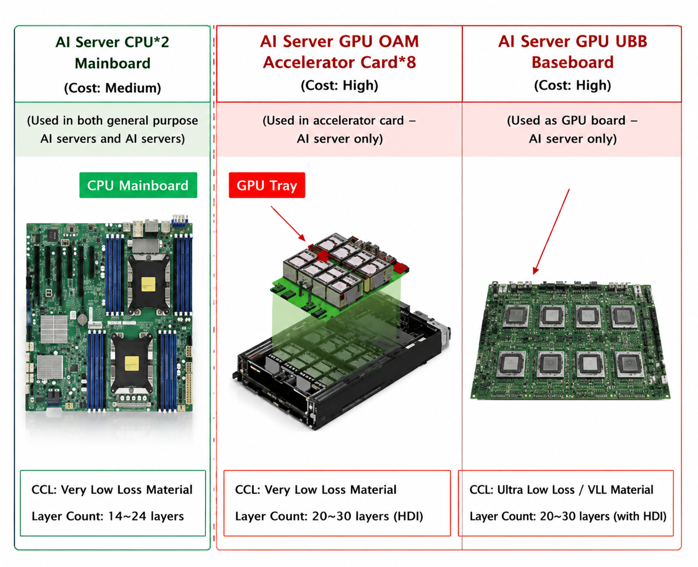
(Figure 1: NVIDIA GB200 utilizes multi-layer HDI PCBs)
The Via-Plugging Dilemma in High-Density Computing
Although HDI PCBs serve as the physical backbone of modern AI computing, they are reaching a critical material bottleneck. HDI PCBs rely heavily on complex micro-via architectures (through, blind, and buried vias). However, traditional via-plugging materials are struggling to keep up with high-power requirements:
- Traditional Resin Plugging: Acts as a thermal and electrical barrier, severely choking heat dissipation along the vertical pathway.
- Transient Liquid Phase Sintering (TLPS): While offering better conductivity, TLPS pastes frequently suffer from voids and micro-cracks during reflow soldering due to thermal stress mismatches, creating significant reliability risks.
In an industry where AI hardware undergoes iterative cycles every few months, hardware engineers urgently require a via-fill material that delivers exceptional thermal and electrical conductivity alongside rock-solid stability.
To address this challenge, Joinspire has launched the JL-CS-F01 via-plugging copper paste. Currently undergoing validation with leading domestic PCB manufacturers, this breakthrough material provides a high-reliability solution for next-generation HDI designs.
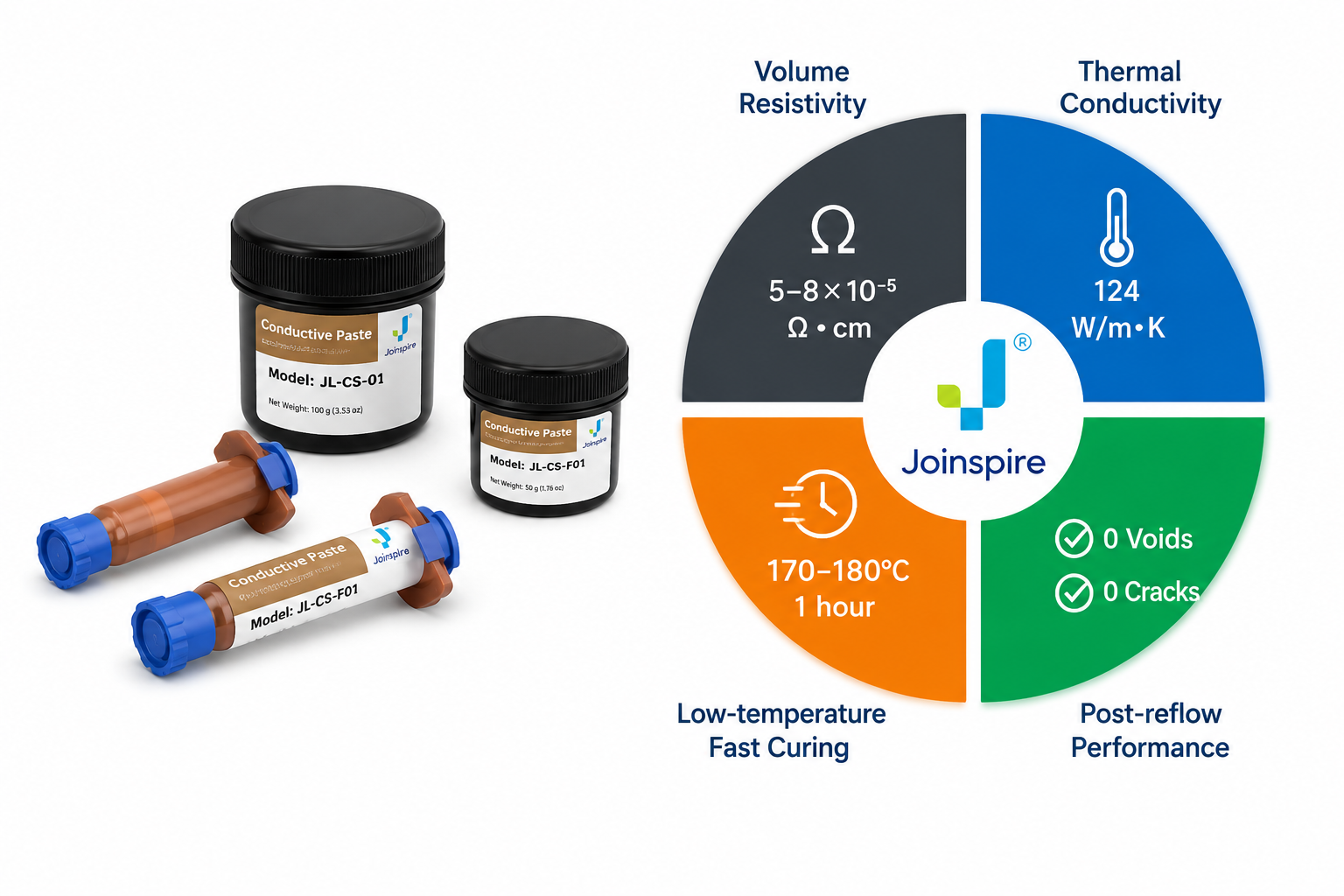
(Figure 2: Key technical features and advantages of Joinspire JL-CS-F01 via-plugging copper paste)
Key Technological Breakthroughs of JL-CS-F01
1. Ultra-Low Resistivity & Superior Thermal Conductivity
While traditional resin plugging behaves like an thermal barrier, Joinspire JL-CS-F01 completely overturns this paradigm. It is not a mere resin modification, but a fully functional conductive paste:
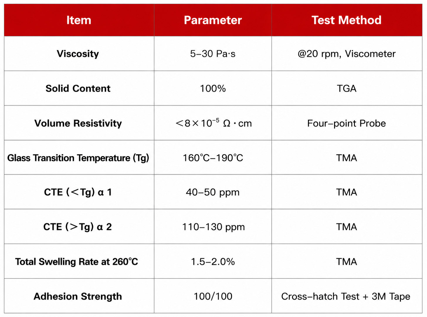
- Volume Resistivity (5–8 × 10⁻⁵ Ω·cm): Enables seamless electrical current flow across multi-layer substrates, significantly reducing line losses and heat generation.
- Thermal Conductivity (124 W/m·K): Creates an “expressway” for vertical heat transport directly beneath high-power AI chips, introducing an entirely new thermal management dimension for accelerator card designers.
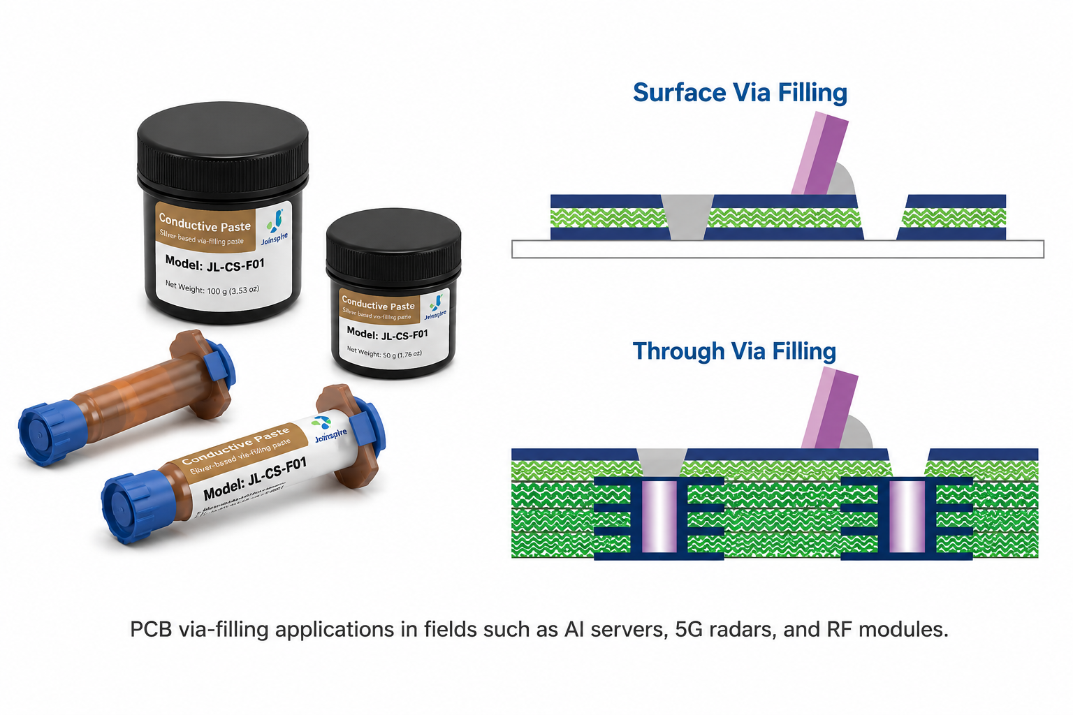
2. Low-Temperature Fast Curing & Excellent Processability
Joinspire JL-CS-F01 offers an exceptionally wide process window:
- Fast Curing (170°C–180°C for 1 Hour): Significantly boosts manufacturing throughput while minimizing thermal stress on delicate substrates.
- Precision CTE Matching: Through controlled volumetric shrinkage, JL-CS-F01 achieves an optimized Coefficient of Thermal Expansion (CTE) match with FR-4 and high-frequency laminates. Whether applied via dispensing or screen printing, it ensures full, dense via-plugging without slump or voiding.
3. Tested for Reliability: 12 Reflow Cycles with Zero Voids or Cracks
Material performance must extend beyond laboratory conditions and withstand extreme operational thermal cycles. During simulated manufacturing tests consisting of 12 continuous reflow cycles, Joinspire JL-CS-F01 demonstrated:
- 0 Voids
- 0 Micro-cracks
- 100% Structural Integrity
This level of thermal stability ensures that internal interconnects remain rock-solid under the continuous thermal cycling typical of high-load AI server operations.
4. Superior Process Flexibility: Solderable Cured Surface
To streamline downstream manufacturing, the cured surface of Joinspire JL-CS-F01 supports direct soldering. This feature gives PCB layout engineers unmatched routing and assembly flexibility—truly achieving a material that “fills densely, conducts reliably, and solders seamlessly.”
Conclusion
The race for AI hardware supremacy extends beyond silicon fabrication; it depends equally on breakthroughs in underlying substrate materials.
If high-performance GPUs represent the “brain” of AI computing and HDI PCBs form the “neural network,” then Joinspire JL-CS-F01 via-plugging copper paste acts as the crucial catalyst linking these nodes together. By solving the challenges of high frequency, high speed, and extreme heat, Joinspire is empowering the next generation of high-density electronic interconnects.
Ready to innovate with us?
Contact our team to learn how our advanced materials can transform your manufacturing.